TSMC To Start 2nm Trials This Year, Mass Production In 2025
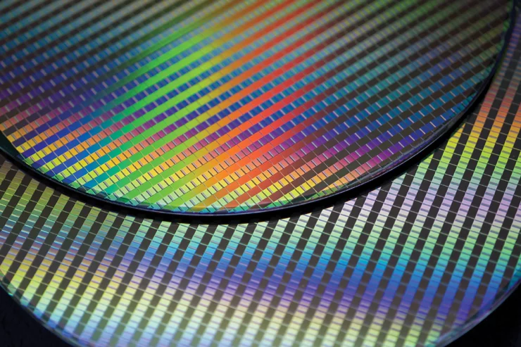
TSMC is stated to start the trials of its 2nm production node, to be used in latest CPU and GPU, this year. Accelerated trials will happen next year. Mass production to start in 2025.
These days, TSMC has become world’s chip manufacturing powerhouse. AMD, Nvidia, Qualcomm, Broadcom and even Intel these days for their Arc GPUs, ask TSMC to make chips for them.
These companies design the chips and Taiwan based TSMC manufacturers them. The reason is simple, TSMC has the latest tech, capacity and ability to do so in a grand manner.
Currently, TSMC is delivering chips made on the 3nm node. Some months ago, we reported how TSMC is going to start the production of it’s 1nm chips in 2028.
But what about 2nm. TSMC is unlikely to jump from 3nm to 1nm directly. That’s not going to happen, as the tech required for 1nm is too complex.
This is where 2nm comes in. Till now, we had no information about when TSMC will start the production of 2nm wafers. Now we do.
2nm Trial This Year, Mass Production Two Years Later
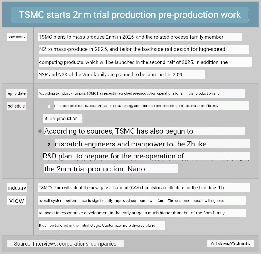
United Daily News reports (translated) that TSMC is in a hurry to start the trial production of 2nm wafers. It has recently started the pre-production of the chips.
Such is the speed that it is expected that TSMC is going to start a small scale trial production of the 2nm chips this year itself. Which is a big surprise.
The report says that the trial will produce 1,000 pieces this year. By pieces, we guess it means complete 300 mm sized wafers.
By next year, TSMC will start producing the chips at a relatively larger level. However, the mass production of 2nm wafers is expected only two years later, in 2025.
Additionally, N2P and N2X upgrades to the 2nm process are expected to launch by 2026.
Tech To Be Used In TSMC 2nm

The article mentions that TSMC is going to use gate-all-around (GAA) architecture for its 2nm node transistors.
Interestingly, Samsung has started mass production of GAA based 3nm chips a year ago.
Intel isn’t far behind with GAA, either. It has named it RibbonFET and it is going to start mass-producing transistors to be used in their CPUs based on RibbonFET in the first half of next year. Intel will use this in their 20A (2nm node), which for now looks more advanced than TSMC’s 2nm node.
TSMC’s 2nm node is also going to use backside power delivery mechanism, which is said to improve the performance of transistors while using lesser power.
Here too, TSMC is competing with Intel. Just a day ago, Intel displayed what it calls PowerVia, a backside power delivery mechanism. Intel claims it provides over 90% cell utilization and over 6% improvement in frequency.
The report on TSMC concludes by mentioning how TSMC will use Nvidia’s powerful servers to manufacture chips on the 2nm. Something that TSMC has worked with Nvidia for four long years.
Either way. TSMC claims that their 2nm node will provide 1.15x density over N3E, which is its most advanced node on 3nm. It also claims their 2nm process will provide 15% speed improvement over same power usage and will use 30% less power at same speeds.
Price Increase
The big problem with TSMC however is the price. From years, it is increasing the prices of its wafers. Digitimes is reporting (via Tom’s Hardware) that TSMC intends to increase the prices further by up to 6% next year.
So yes. Intel and Samsung aren’t far behind. But in TSMC has numbers, capacity, ability and most importantly, customers like Nvidia.
Customers who are prepared to pay huge amounts of money and book the capacities of TSMC, no matter how much they charge.
Customers are who want TSMC to deliver the latest tech possible quickly. Looks like TSMC is trying its best to do that.
